Semiconductor Inspection and Measurement / Flaw Detection Applications
VisionGauge® machine vision software and systems are well-suited to various semiconductor inspection and measurement applications, including polishing pad inspection, hybrid inspection, epoxy underfill measurement, substrate inspection, wafer defect detection, line, trace width and other semiconductor feature measurements, and much more.
Semiconductor Epoxy Underfill Measurement
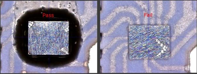
In the electronic device manufacturing industry Epoxy resin is used as an adhesive or as an insulator on the component layer of PCB boards. Inspecting the presence and assuring the right amount of epoxy is present is a very important part of the quality assurance process. Our VisiongGauge® Online Automated Optical Inspection (AOI) systems are being employed to automatically detect the presence of semiconductor epoxy underfill on electronic devices, between a high-density circuit and its substrate, during the assembly process. VisionGauge® OnLine also accurately measures the under-fill's "footprint" (i.e. maximum dimensions along the X and Y axes). This is carried out in-process, right after the dispensing and placement operations.
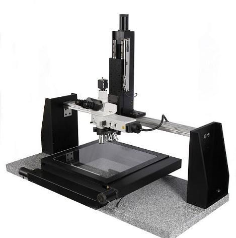
These systems are highly capable when dealing with great magnification, and they posses accuracy up to 0.1 micron. These systems are fully automated and can be programmed to move in a three-dimensional set of coordinates. Furthermore, you can use the system manually with the help of a joystick through our easy to use VisionGauge® Online machine vision software.
VisionGauge® Online includes many features to make your automated epoxy measurement effective and efficient. You can easily create your own programs using VisionGauge® OnLine to teach the machine how to perform the measurements automatically. The software is capable of auto-focus, which provides you with accurate and highly repeatable results. In addition, these systems are available with computer controlled illumination reflected or direct lighting.
You can automatically export/save measurement and inspection results, control input and output signals based on inspection results, and even automatically create reports with this information. For more information about how VisionGauge® software and systems perform wafer measurements, semiconductor inspection, or flaw detection, please contact us.
Semiconductor Wafer Inspection and Automated Flaw Detection
Our VisionGauge® Online Automated Optical Inspections Systems (AOI Systems) are high accuracy tools for automated defect detection, measurement, and inspection. In the semiconductor manufacturing industry, thorough final inspection of wafers is a critical part of the production process; our AOI systems are designed to help you obtain the best results possible.
These systems are highly capable when dealing with great magnification with an accuracy up to 0.1 micron. These systems are fully automated and can be programmed to move in a three-dimensional set of coordinates. Optionally, you can use the system manually with the help of a joystick through our versatile VisionGauge® Online machine vision software.
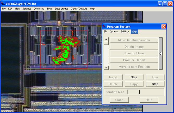
VisionGauge® Online includes many features to make your automated flaw detection and semiconductor wafer inspection effective and efficient. Easily create your own programs using VisionGauge® OnLine to teach the machine how to perform the inspection. The software is capable of auto-focus and repeatable, computer controlled illumination intensity with transmitted or reflected illumination, which provides you with accurate and precise results. VisionGauge® Online's auto-scan tool is capable of automatically detecting any flaws on the wafer.
You can automatically save measurement and inspection results, save the images for "Pass" or "Fail" parts of the wafer, manipulate input and output signals based on inspection results, and even automatically create detailed reports with this information.
 In one example, VisionGauge® OnLine is applied in semiconductor defect detection by a printer manufacturer to automatically review stored sequences of images and find any defects that might be contained in the images. In this application, the images are of various semiconductor products produced by this manufacturer. VisionGauge® OnLine can be asked to handle sequences of up to 22,000 images in a single run. This is not a problem for VisionGauge® OnLine as there are no limits to the number of images that it can handle. VisionGauge® OnLine is initially trained using "known good" images of the various types of products to inspect. It is then automatically detects defects and non-conformities. Images that VisionGauge® OnLine characterizes as "good" are ignored and "bad" images are collected for operator review and corrective action. Statistics of VisionGauge® OnLine’s analysis are also collected (i.e. defect rate, etc…)
Information is also available about more recent applications solved with our fleet of VisionGauge® Digital Optical Comparators.