
The VisionGauge® High-Accuracy Inspection & Measurement Systems are an excellent solution both wafer and die level inspection of semiconductors. These systems have extensive measurement, pattern matching, and defect detection tools and they are extremely easy to program. This makes them especially well-suited to applications involving small lots and high changeover (such as R&D, prototyping, and small-batch-production applications). In many cases, they can be programmed using the part’s CAD data directly.

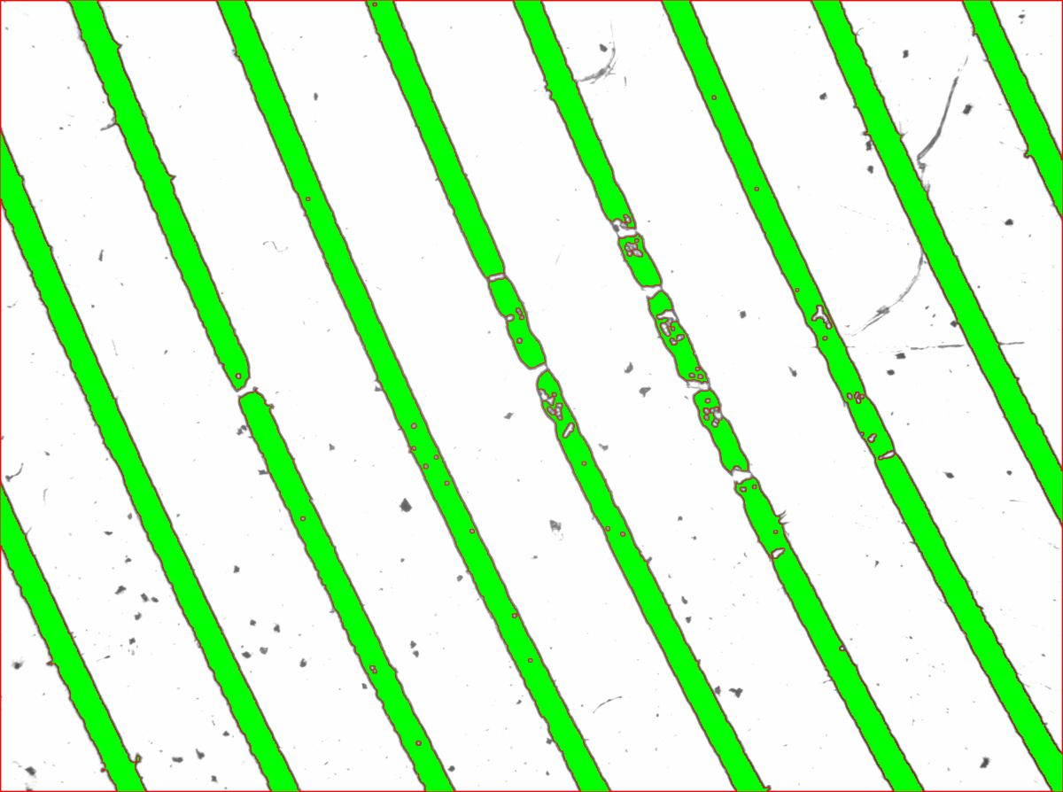
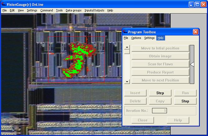
VisionGauge® systems can automatically detect a wide range of physical & surface defects including: cracks & fractures, scratches, pits, chipping, contamination, particles, foreign materials, delamination, voids, pattern defects, bridges and shorts, feature misalignment, etc.
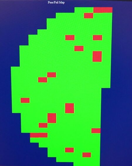
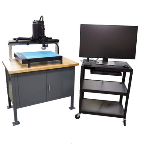
We offer many different system configurations that all run the same VisionGauge® software. VisionGauge® has a very intuitive graphical user interface and is extremely easy to use. It has extensive data analysis, exchange, collection & reporting tools. Results can also be presented graphically (for example: an interactive “defect map” can be displayed).
VisionGauge® systems are flexible, widely applicable, and cost-effective solutions for automated defect detection on semiconductors with high precision.

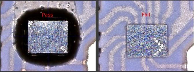
In the electronic device manufacturing industry Epoxy resin is used as an adhesive or as an insulator on the component layer of PCB boards. Inspecting the presence and assuring the right amount of epoxy is present is an important part of the quality assurance process. VisiongGauge® systems are being employed to automatically detect the presence of semiconductor epoxy underfill on electronic devices, between a high-density circuit and its substrate, during the assembly process. VisionGauge® also accurately measures the under-fill’s “footprint” (i.e. maximum dimensions along the X and Y axes). This is carried out in-process, right after the dispensing and placement operations.
Automated epoxy measurement is effective and efficient with VisionGauge® Online with powerful features. Customize programs to teach the machine how to perform measurements automatically with auto-focus for accurate and highly repeatable results. Automatically export/save measurement and inspection results, control input and output signals based on inspection results, and even automatically create reports with this information.
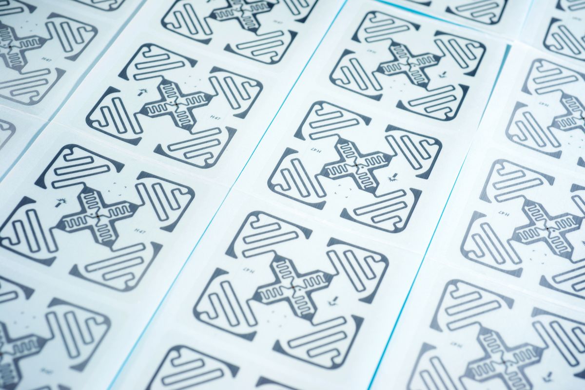
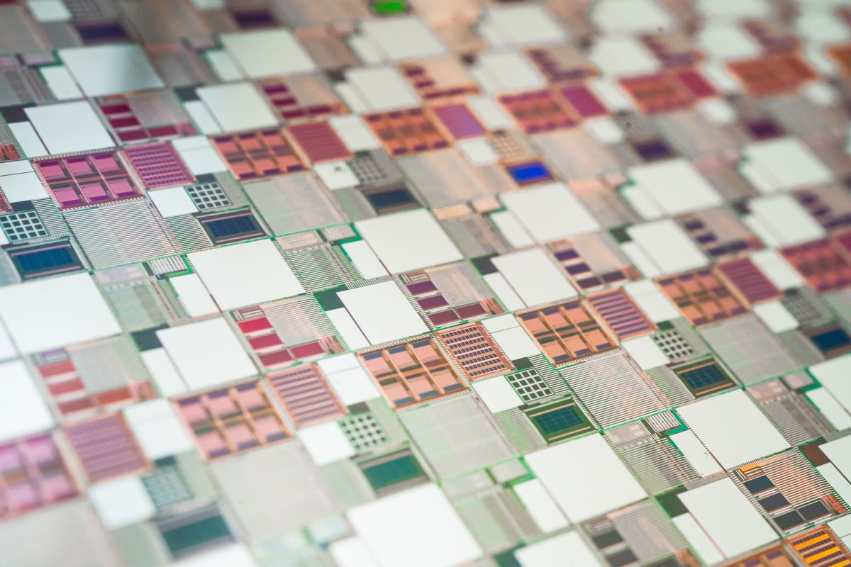
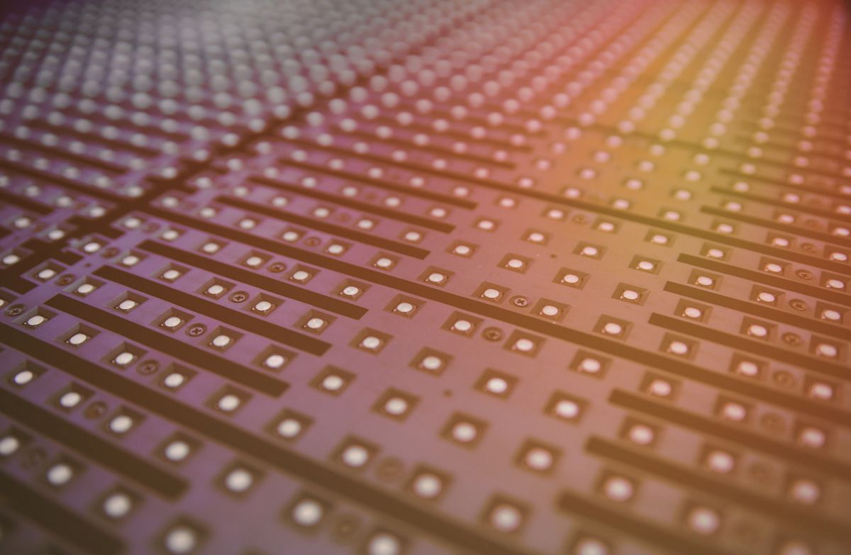
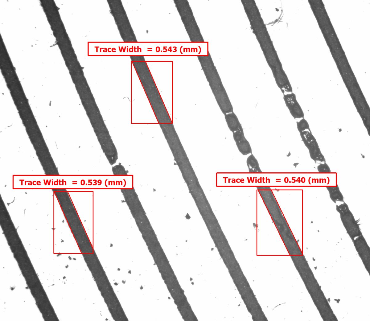
In the semiconductor manufacturing industry, thorough final inspection of wafers is a critical part of the production process. VisionGauge® inspection and measurement systems are high accuracy tools for automated defect detection, measurement, and inspection – designed to provide the highest quality results. Create automated stage-based inspection programs for multiple parts quickly and easily with pattern matching and comparison steps to reliably detect flaws, contamination, and imperfections on wafers, semiconductors, and other parts.
In one example, VisionGauge® is applied in semiconductor defect detection by a printer manufacturer to automatically review stored sequences of images and find any defects that might be contained in the images. In this application, the images are of various semiconductor products produced by this manufacturer. VisionGauge® can be asked to handle sequences of up to 22,000 images in a single run. This is not a problem for VisionGauge® as there are no limits to the number of images that it can handle. VisionGauge® is initially trained using “known good” images of the various types of products to inspect. It then automatically detects defects and non-conformities. Images that VisionGauge® characterizes as “good” or “Go” are ignored and “bad” or “No Go” images are collected for operator review and corrective action. Statistics of VisionGauge®’s analysis are also collected (i.e. defect rate, etc.)
VisionGauge®
A .pdf version of this VisionGauge® Digital Optical Comparator Application Note is available to download. Also, learn more about other applications our systems are regularly being used to solve.
Contact us with more information about your application and to arrange a demo of our systems.

Are you interested in streamlining your inspection process with VisionGauge® Digital Optical Comparators and optical measuring systems? As your vision inspection system manufacturer, we’re available to provide support at any time, so browse our selection of products or contact us online today.
Learn More